|
Cache hierarchyCache hierarchy, or multi-level cache, is a memory architecture that uses a hierarchy of memory stores based on varying access speeds to cache data. Highly requested data is cached in high-speed access memory stores, allowing swifter access by central processing unit (CPU) cores. Cache hierarchy is a form and part of memory hierarchy and can be considered a form of tiered storage.[1] This design was intended to allow CPU cores to process faster despite the memory latency of main memory access. Accessing main memory can act as a bottleneck for CPU core performance as the CPU waits for data, while making all of main memory high-speed may be prohibitively expensive. High-speed caches are a compromise allowing high-speed access to the data most-used by the CPU, permitting a faster CPU clock.[2]  BackgroundIn the history of computer and electronic chip development, there was a period when increases in CPU speed outpaced the improvements in memory access speed.[3] The gap between the speed of CPUs and memory meant that the CPU would often be idle.[4] CPUs were increasingly capable of running and executing larger amounts of instructions in a given time, but the time needed to access data from main memory prevented programs from fully benefiting from this capability.[5] This issue motivated the creation of memory models with higher access rates in order to realize the potential of faster processors.[6] This resulted in the concept of cache memory, first proposed by Maurice Wilkes, a British computer scientist at the University of Cambridge in 1965. He called such memory models "slave memory".[7] Between roughly 1970 and 1990, papers and articles by Anant Agarwal, Alan Jay Smith, Mark D. Hill, Thomas R. Puzak, and others discussed better cache memory designs. The first cache memory models were implemented at the time, but even as researchers were investigating and proposing better designs, the need for faster memory models continued. This need resulted from the fact that although early cache models improved data access latency, with respect to cost and technical limitations it was not feasible for a computer system's cache to approach the size of main memory. From 1990 onward, ideas such as adding another cache level (second-level), as a backup for the first-level cache were proposed. Jean-Loup Baer, Wen-Hann Wang, Andrew W. Wilson, and others have conducted research on this model. When several simulations and implementations demonstrated the advantages of two-level cache models, the concept of multi-level caches caught on as a new and generally better model of cache memories. Since 2000, multi-level cache models have received widespread attention and are currently implemented in many systems, such as the three-level caches that are present in Intel's Core i7 products.[8] Multi-level cacheAccessing main memory for each instruction execution may result in slow processing, with the clock speed depending on the time required to find and fetch the data. In order to hide this memory latency from the processor, data caching is used.[9] Whenever the data is required by the processor, it is fetched from the main memory and stored in the smaller memory structure called a cache. If there is any further need of that data, the cache is searched first before going to the main memory.[10] This structure resides closer to the processor in terms of the time taken to search and fetch data with respect to the main memory.[11] The advantages of using cache can be proven by calculating the average access time (AAT) for the memory hierarchy with and without the cache.[12] Average access time (AAT)Caches, being small in size, may result in frequent misses – when a search of the cache does not provide the sought-after information – resulting in a call to main memory to fetch data. Hence, the AAT is affected by the miss rate of each structure from which it searches for the data.[13] AAT for main memory is given by Hit time main memory. AAT for caches can be given by
The hit time for caches is less than the hit time for the main memory, so the AAT for data retrieval is significantly lower when accessing data through the cache rather than main memory.[14] Trade-offsWhile using the cache may improve memory latency, it may not always result in the required improvement for the time taken to fetch data due to the way caches are organized and traversed. For example, direct-mapped caches that are the same size usually have a higher miss rate than fully associative caches. This may also depend on the benchmark of the computer testing the processor and on the pattern of instructions. But using a fully associative cache may result in more power consumption, as it has to search the whole cache every time. Due to this, the trade-off between power consumption (and associated heat) and the size of the cache becomes critical in the cache design.[13] Evolution In the case of a cache miss, the purpose of using such a structure will be rendered useless and the computer will have to go to the main memory to fetch the required data. However, with a multiple-level cache, if the computer misses the cache closest to the processor (level-one cache or L1) it will then search through the next-closest level(s) of cache and go to main memory only if these methods fail. The general trend is to keep the L1 cache small and at a distance of 1–2 CPU clock cycles from the processor, with the lower levels of caches increasing in size to store more data than L1, hence being more distant but with a lower miss rate. This results in a better AAT.[15] The number of cache levels can be designed by architects according to their requirements after checking for trade-offs between cost, AATs, and size.[16][17] Performance gainsWith the technology-scaling that allowed memory systems able to be accommodated on a single chip, most modern day processors have up to three or four cache levels.[18] The reduction in the AAT can be understood by this example, where the computer checks AAT for different configurations up to L3 caches. Example: main memory = 50 ns, L1 = 1 ns with 10% miss rate, L2 = 5 ns with 1% miss rate, L3 = 10 ns with 0.2% miss rate.
Disadvantages
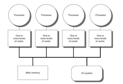
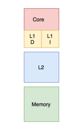
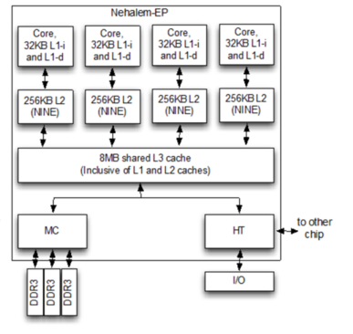
Properties Banked versus unifiedIn a banked cache, the cache is divided into a cache dedicated to instruction storage and a cache dedicated to data. In contrast, a unified cache contains both the instructions and data in the same cache.[22] During a process, the L1 cache (or most upper-level cache in relation to its connection to the processor) is accessed by the processor to retrieve both instructions and data. Requiring both actions to be implemented at the same time requires multiple ports and more access time in a unified cache. Having multiple ports requires additional hardware and wiring, leading to a significant structure between the caches and processing units.[23] To avoid this, the L1 cache is often organized as a banked cache which results in fewer ports, less hardware, and generally lower access times.[13] Modern processors have split caches, and in systems with multilevel caches higher level caches may be unified while lower levels split.[24] Inclusion policies Whether a block present in the upper cache layer can also be present in the lower cache level is governed by the memory system's inclusion policy, which may be inclusive, exclusive or non-inclusive non-exclusive (NINE).[citation needed] With an inclusive policy, all the blocks present in the upper-level cache have to be present in the lower-level cache as well. Each upper-level cache component is a subset of the lower-level cache component. In this case, since there is a duplication of blocks, there is some wastage of memory. However, checking is faster.[citation needed] Under an exclusive policy, all the cache hierarchy components are completely exclusive, so that any element in the upper-level cache will not be present in any of the lower cache components. This enables complete usage of the cache memory. However, there is a high memory-access latency.[25] The above policies require a set of rules to be followed in order to implement them. If none of these are forced, the resulting inclusion policy is called non-inclusive non-exclusive (NINE). This means that the upper-level cache may or may not be present in the lower-level cache.[21] Write policiesThere are two policies which define the way in which a modified cache block will be updated in the main memory: write through and write back.[citation needed] In the case of write through policy, whenever the value of the cache block changes, it is further modified in the lower-level memory hierarchy as well.[26] This policy ensures that the data is stored safely as it is written throughout the hierarchy. However, in the case of the write back policy, the changed cache block will be updated in the lower-level hierarchy only when the cache block is evicted. A "dirty bit" is attached to each cache block and set whenever the cache block is modified.[27] During eviction, blocks with a set dirty bit will be written to the lower-level hierarchy. Under this policy, there is a risk for data-loss as the most recently changed copy of a datum is only stored in the cache and therefore some corrective techniques must be observed. In case of a write where the byte is not present in the cache block, the byte may be brought to the cache as determined by a write allocate or write no-allocate policy.[28] Write allocate policy states that in case of a write miss, the block is fetched from the main memory and placed in the cache before writing.[29] In the write no-allocate policy, if the block is missed in the cache it will write in the lower-level memory hierarchy without fetching the block into the cache.[30] The common combinations of the policies are "write back, write allocate" and "write through, write no-allocate". Shared versus private A private cache is assigned to one particular core in a processor, and cannot be accessed by any other cores. In some architectures, each core has its own private cache; this creates the risk of duplicate blocks in a system's cache architecture, which results in reduced capacity utilization. However, this type of design choice in a multi-layer cache architecture can also be good for a lower data-access latency.[28][31][32] A shared cache is a cache which can be accessed by multiple cores.[33] Since it is shared, each block in the cache is unique and therefore has a larger hit rate as there will be no duplicate blocks. However, data-access latency can increase as multiple cores try to access the same cache.[34] In multi-core processors, the design choice to make a cache shared or private impacts the performance of the processor.[35] In practice, the upper-level cache L1 (or sometimes L2)[36][37] is implemented as private and lower-level caches are implemented as shared. This design provides high access rates for the high-level caches and low miss rates for the lower-level caches.[35] Recent implementation models Intel Xeon Emerald Rapids (2024)Up 64 core:
Intel i5 Raptor Lake-HX (2024)6 core (performance| efficiency):
AMD EPYC 9684X (2023)96 core:
Apple M1 Ultra (2022)20 core (4:1 "performance" core | "efficiency" core):
AMD Ryzen 7000 (2022)6 to 16 core:
AMD Zen 2 microarchitecture (2019)
AMD Zen microarchitecture (2017)
Intel Kaby Lake microarchitecture (2016)
Intel Broadwell microarchitecture (2014)
IBM POWER7 (2010)
See also
References
|
