|
Gallium phosphide
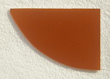
Gallium phosphide (GaP), a phosphide of gallium, is a compound semiconductor material with an indirect band gap of 2.24 eV at room temperature. Impure polycrystalline material has the appearance of pale orange or grayish pieces. Undoped single crystals are orange, but strongly doped wafers appear darker due to free-carrier absorption. It is odorless and insoluble in water. GaP has a microhardness of 9450 N/mm2, a Debye temperature of 446 K (173 °C), and a thermal expansion coefficient of 5.3 ×10⁻⁶ K−1 at room temperature.[4] Sulfur, silicon or tellurium are used as dopants to produce n-type semiconductors. Zinc is used as a dopant for the p-type semiconductor. Gallium phosphide has applications in optical systems.[6][7][8] Its static dielectric constant is 11.1 at room temperature.[2] Its refractive index varies between ~3.2 and 5.0 across the visible range, which is higher than in most other semiconducting materials.[3] In its transparent range, its index is higher than almost any other transparent material, including gemstones such as diamond, or non-oxide lenses such as zinc sulfide. Light-emitting diodesGallium phosphide has been used in the manufacture of low-cost red, orange, and green light-emitting diodes (LEDs) with low to medium brightness since the 1960s. It is used standalone or together with gallium arsenide phosphide. Pure GaP LEDs emit green light at a wavelength of 555 nm. Nitrogen-doped GaP emits yellow-green (565 nm) light, zinc oxide doped GaP emits red (700 nm). Gallium phosphide is transparent for yellow and red light, therefore GaAsP-on-GaP LEDs are more efficient than GaAsP-on-GaAs. Crystal growthAt temperatures above ~900 °C, gallium phosphide dissociates and the phosphorus escapes as a gas. In crystal growth from a 1500 °C melt (for LED wafers), this must be prevented by holding the phosphorus in with a blanket of molten boric oxide in inert gas pressure of 10–100 atmospheres. The process is called liquid encapsulated Czochralski (LEC) growth, an elaboration of the Czochralski process used for silicon wafers. References
Cited sources
External links
|
||||||||||||||||||||||||||||||||||||||||||||||||||||||||||||||||||||||||||||||||||||||||


