|
Intel 80286
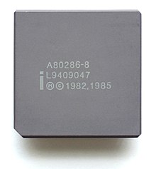
The Intel 80286[4] (also marketed as the iAPX 286[5] and often called Intel 286) is a 16-bit microprocessor that was introduced on February 1, 1982. It was the first 8086-based CPU with separate, non-multiplexed address and data buses and also the first with memory management and wide protection abilities. The 80286 used approximately 134,000 transistors in its original nMOS (HMOS) incarnation and, just like the contemporary 80186,[6] it can correctly execute most software written for the earlier Intel 8086 and 8088 processors.[7] The 80286 was employed for the IBM PC/AT, introduced in 1984, and then widely used in most PC/AT compatible computers until the early 1990s. In 1987, Intel shipped its five-millionth 80286 microprocessor.[8] History and performance Intel's first 80286 chips were specified for a maximum clockrate of 5, 6 or 8 MHz and later releases for 12.5 MHz. AMD and Harris later produced 16 MHz, 20 MHz and 25 MHz parts, respectively. Intel, Intersil and Fujitsu also designed fully static CMOS versions of Intel's original depletion-load nMOS implementation, largely aimed at battery-powered devices. Intel's CMOS version of the 80286 was the 80C286. On average, the 80286 was said to have a speed of about 0.21 instructions per clock on "typical" programs,[9] although it could be significantly faster on optimized code and in tight loops, as many instructions could execute in 2 clock cycles each. The 6 MHz, 10 MHz, and 12 MHz models were reportedly measured to operate at 0.9 MIPS, 1.5 MIPS, and 2.66 MIPS respectively.[10] The later E-stepping level of the 80286 was free of the several significant errata that caused problems for programmers and operating-system writers in the earlier B-step and C-step CPUs (common in the AT and AT clones). This E-2 stepping part may have been available in later 1986.[11] Intel second sourced this microprocessor to Fujitsu Limited in about 1985.[12] Variants
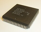
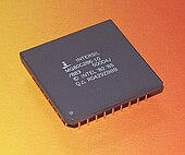
Architecture  Intel expected the 286 to be used primarily in industrial automation, transaction processing, and telecommunications, instead of in personal computers.[16] The CPU was designed for multi-user systems with multitasking applications, including communications (such as automated PBXs) and real-time process control. It had 134,000 transistors and consisted of four independent units: the address unit, bus unit, instruction unit, and execution unit, organized into a loosely coupled (buffered) pipeline, just as in the 8086. It was produced in a 68-pin package, including PLCC (plastic leaded chip carrier), LCC (leadless chip carrier) and PGA (pin grid array) packages.[17] The performance increase of the 80286 over the 8086 (or 8088) could be more than 100% per clock cycle in many programs (i.e., a doubled performance at the same clock speed). This was a large increase, fully comparable to the speed improvements seven years later when the i486 (1989) or the original Pentium (1993) were introduced. This was partly due to the non-multiplexed address and data buses, but mainly to the fact that address calculations (such as base+index) were less expensive. They were performed by a dedicated unit in the 80286, while the older 8086 had to do effective address computation using its general ALU, consuming several extra clock cycles in many cases. Also, the 80286 was more efficient in the prefetch of instructions, buffering, execution of jumps, and in complex microcoded numerical operations such as MUL/DIV than its predecessor.[18] The 80286 included, in addition to all of the 8086 instructions, all of the new instructions of the 80186: ENTER, LEAVE, BOUND, INS, OUTS, PUSHA, POPA, PUSH immediate, IMUL immediate, and immediate shifts and rotates. The 80286 also added new instructions for protected mode: ARPL, CLTS, LAR, LGDT, LIDT, LLDT, LMSW, LSL, LTR, SGDT, SIDT, SLDT, SMSW, STR, VERR, and VERW. Some of the instructions for protected mode can (or must) be used in real mode to set up and switch to protected mode, and a few (such as SMSW and LMSW) are useful for real mode itself. The Intel 80286 had a 24-bit address bus and as such had a 16 MB physical address space, compared to the 1 MB address space of prior x86 processors. It was the first x86 processor to support virtual memory supporting up to 1 GB via segmentation.[19] However, memory cost and the initial rarity of software using the memory above 1 MB meant that until late in its production, 80286 computers rarely shipped with more than 1 MB of RAM.[18] Additionally, there was a performance penalty involved in accessing extended memory from real mode as noted below. Features   Protected modeThe 286 was the first of the x86 CPU family to support protected virtual-address mode, commonly called "protected mode". In addition, it was the first commercially available microprocessor with on-chip memory management unit (MMU) capabilities (systems using the contemporaneous Motorola 68010 and NS320xx could be equipped with an optional MMU controller). This would allow IBM compatibles to have advanced multitasking OSes for the first time and compete in the Unix-dominated[citation needed] server/workstation market. Several additional instructions were introduced in the protected mode of 80286, which are helpful for multitasking operating systems. Another important feature of 80286 is the prevention of unauthorized access. This is achieved by:
In 80286 (and in its co-processor Intel 80287), arithmetic operations can be performed on the following different types of numbers:
By design, the 286 could not revert from protected mode to the basic 8086-compatible real address mode ("real mode") without a hardware-initiated reset. In the PC/AT introduced in 1984, IBM added external circuitry, as well as specialized code in the ROM BIOS and the 8042 keyboard microcontroller to enable software to cause the reset, allowing real-mode reentry while retaining active memory and returning control to the program that initiated the reset. (The BIOS is necessarily involved because it obtains control directly whenever the CPU resets.) Though it worked correctly, the method imposed a huge performance penalty. In theory, real-mode applications could be directly executed in 16-bit protected mode if certain rules (newly proposed with the introduction of the 80286) were followed; however, as many DOS programs did not conform to those rules, protected mode was not widely used until the appearance of its successor, the 32-bit Intel 80386, which was designed to go back and forth between modes easily and to provide an emulation of real mode within protected mode. When Intel designed the 286, it was not designed to be able to multitask real-mode applications; real mode was intended to be a simple way for a bootstrap loader to prepare the system and then switch to protected mode; essentially, in protected mode the 80286 was designed to be a new processor with many similarities to its predecessors, while real mode on the 80286 was offered for smaller-scale systems that could benefit from a more advanced version of the 80186 CPU core, with advantages such as higher clock rates, faster instruction execution (measured in clock cycles), and unmultiplexed buses, but not the 24-bit (16 MB) memory space. To support protected mode, new instructions have been added: ARPL, VERR, VERW, LAR, LSL, SMSW, SGDT, SIDT, SLDT, STR, LMSW, LGDT, LIDT, LLDT, LTR, CLTS. There are also new exceptions (internal interrupts): invalid opcode, coprocessor not available, double fault, coprocessor segment overrun, stack fault, segment overrun/general protection fault, and others only for protected mode. OS supportThe protected mode of the 80286 was not routinely utilized in PC applications until many years after its release, in part because of the high cost of adding extended memory to a PC, but also because of the need for software to support the large user base of 8086 PCs. For example, in 1986 the only program that made use of it was VDISK, a RAM disk driver included with PC DOS 3.0 and 3.1. A DOS could utilize the additional RAM available in protected mode (extended memory) either via a BIOS call (INT 15h, AH=87h), as a RAM disk, or as emulation of expanded memory.[18] The difficulty lay in the incompatibility of older real-mode DOS programs with protected mode. They simply could not natively run in this new mode without significant modification. In protected mode, memory management and interrupt handling were done differently than in real mode. In addition, DOS programs typically would directly access data and code segments that did not belong to them, as real mode allowed them to do without restriction; in contrast, the design intent of protected mode was to prevent programs from accessing any segments other than their own unless special access was explicitly allowed. While it was possible to set up a protected-mode environment that allowed all programs access to all segments (by putting all segment descriptors into the Global Descriptor Table (GDT) and assigning them all the same privilege level), this undermined nearly all of the advantages of protected mode except the extended (24-bit) address space. The choice that OS developers faced was either to start from scratch and create an OS that would not run the vast majority of the old programs, or to come up with a version of DOS that was slow and ugly (i.e., ugly from an internal technical viewpoint) but would still run a majority of the old programs. Protected mode also did not provide a significant enough performance advantage over the 8086-compatible real mode to justify supporting its capabilities; actually, except for task switches when multitasking, it yielded only a performance disadvantage, by slowing down many instructions through a litany of added privilege checks. In protected mode, registers were still 16-bit, and the programmer was still forced to use a memory map composed of 64 kB segments, just like in real mode.[20] In January 1985, Digital Research previewed the Concurrent DOS 286 1.0 operating system developed in cooperation with Intel. The product would function strictly as an 80286 native-mode (i.e. protected-mode) operating system, allowing users to take full advantage of the protected mode to perform multi-user, multitasking operations while running 8086 emulation.[21][22][23] This worked on the B-1 prototype step of the chip, but Digital Research discovered problems with the emulation on the production level C-1 step in May, which would not allow Concurrent DOS 286 to run 8086 software in protected mode. The release of Concurrent DOS 286 was delayed until Intel would develop a new version of the chip.[21] In August, after extensive testing on E-1 step samples of the 80286, Digital Research acknowledged that Intel corrected all documented 286 errata, but said that there were still undocumented chip performance problems with the prerelease version of Concurrent DOS 286 running on the E-1 step. Intel said that the approach Digital Research wished to take in emulating 8086 software in protected mode differed from the original specifications. Nevertheless, in the E-2 step, they implemented minor changes in the microcode that would allow Digital Research to run emulation mode much faster.[11] Named IBM 4680 OS, IBM originally chose DR Concurrent DOS 286 as the basis of their IBM 4680 computer for IBM Plant System products and point-of-sale terminals in 1986.[24] Digital Research's FlexOS 286 version 1.3, a derivation of Concurrent DOS 286, was developed in 1986, introduced in January 1987, and later adopted by IBM for their IBM 4690 OS, but the same limitations affected it. The problems led to Bill Gates referring to the 80286 as a "brain-damaged" chip,[25] since it was clear that the new Microsoft Windows environment would not be able to run multiple MS-DOS applications with the 286. It was arguably responsible for the split between Microsoft and IBM, since IBM insisted that OS/2, originally a joint venture between IBM and Microsoft, would run on a 286 (and in text mode). Other operating systems that used the protected mode of the 286 were Microsoft Xenix (around 1984),[26] Coherent,[27] and Minix.[28] These were less hindered by the limitations of the 80286 protected mode because they did not aim to run MS-DOS applications or other real-mode programs. In its successor 80386 chip, Intel enhanced the protected mode to address more memory and also added the separate virtual 8086 mode, a mode within protected mode with much better MS-DOS compatibility, in order to satisfy the diverging needs of the market.[29] Support componentsThis list of bus interface components that connects to Intel 80286 microprocessor.
See also
References
External linksWikimedia Commons has media related to Intel 80286.
|
||||||||||||||||||||||||||||||||||||||||||||||||||||||||||||||||||||||||||||||||||||||||
